Contents
- 🔍 Introduction to Scanning Tunneling Microscopy
- 💡 History of STM: The Nobel Prize Winning Discovery
- 🔬 Principles of Operation: How STM Works
- 📈 Applications of Scanning Tunneling Microscopy
- 🌐 Environmental Variants: STM in Air, Water, and Extreme Temperatures
- 🔍 Imaging and Manipulation of Atoms: The Power of STM
- 🤝 Relationship Between STM and Other Microscopy Techniques
- 📊 Future Developments and Challenges in Scanning Tunneling Microscopy
- 📚 Conclusion: The Impact of Scanning Tunneling Microscopy on Physics and Nanotechnology
- 📊 Topic Intelligence and Key Concepts
- 🌈 Controversy and Debates in the Field of Scanning Tunneling Microscopy
- Frequently Asked Questions
- Related Topics
Overview
Scanning tunneling microscopy (STM) has been a groundbreaking technique since its invention in 1981 by Gerd Binnig and Heinrich Rohrer at IBM Zurich. This method allows for the visualization of surfaces at the atomic level, with a resolution that surpasses traditional microscopy methods. By employing a sharp probe that scans the surface of a material, STM can detect the tunneling current that flows between the probe and the surface, providing detailed topographic images. The impact of STM has been profound, enabling scientists to study surface phenomena, manipulate individual atoms, and explore the properties of nanomaterials. With a Vibe score of 8, STM has opened up new avenues for research in fields like materials science, chemistry, and physics. As researchers continue to push the boundaries of this technology, we can expect significant advancements in our understanding of the nanoscale world, with potential applications in fields like energy storage, catalysis, and quantum computing.
🔍 Introduction to Scanning Tunneling Microscopy
The development of Scanning Tunneling Microscopy (STM) has revolutionized the field of physics and nanotechnology. This technique allows for the imaging of surfaces at the atomic level, enabling scientists to study the properties of materials at the smallest scales. The invention of STM in 1981 by Gerd Binnig and Heinrich Rohrer at IBM Zürich earned them the Nobel Prize in Physics in 1986. Today, STM is a crucial tool in various fields, including materials science and surface science. For more information on the history of STM, visit the IBM website or the Nobel Prize website.
💡 History of STM: The Nobel Prize Winning Discovery
The history of Scanning Tunneling Microscopy (STM) is a fascinating story of innovation and discovery. In 1981, Gerd Binnig and Heinrich Rohrer developed the first STM, which used a sharp conducting tip to sense the surface of materials at the atomic level. This invention earned them the Nobel Prize in Physics in 1986, recognizing the significance of their discovery. The development of STM has been influenced by the work of other scientists, including Richard Feynman, who is known for his work in quantum mechanics. To learn more about the life and work of Richard Feynman, visit the Caltech website.
🔬 Principles of Operation: How STM Works
The principles of operation of Scanning Tunneling Microscopy (STM) are based on the concept of quantum tunneling. In STM, a sharp conducting tip is brought close to the surface of a material, allowing electrons to tunnel through the gap between the tip and the surface. This tunneling current is sensitive to the distance between the tip and the surface, enabling the imaging of surfaces at the atomic level. The resolution of STM is incredibly high, with a depth resolution of 0.01 nm (10 pm) and a lateral resolution of 0.1 nm. To understand the principles of quantum tunneling, visit the Wikipedia page on the topic.
📈 Applications of Scanning Tunneling Microscopy
The applications of Scanning Tunneling Microscopy (STM) are diverse and widespread. In materials science, STM is used to study the properties of materials at the atomic level, including their crystal structure and surface properties. In nanotechnology, STM is used to manipulate individual atoms and molecules, enabling the creation of nanostructures with unique properties. STM is also used in surface science to study the properties of surfaces and interfaces. For more information on the applications of STM, visit the National Institute of Standards and Technology website.
🌐 Environmental Variants: STM in Air, Water, and Extreme Temperatures
While most Scanning Tunneling Microscopy (STM) systems are designed for use in ultra-high vacuum at temperatures approaching absolute zero, variants exist for studies in air, water, and other environments. These variants enable the study of surfaces and materials in a wide range of conditions, from the atmosphere to high-temperature environments. For example, STM in air is used to study the properties of materials in their natural environment, while STM in water is used to study the properties of biological molecules. To learn more about the different variants of STM, visit the Wikipedia page on the topic.
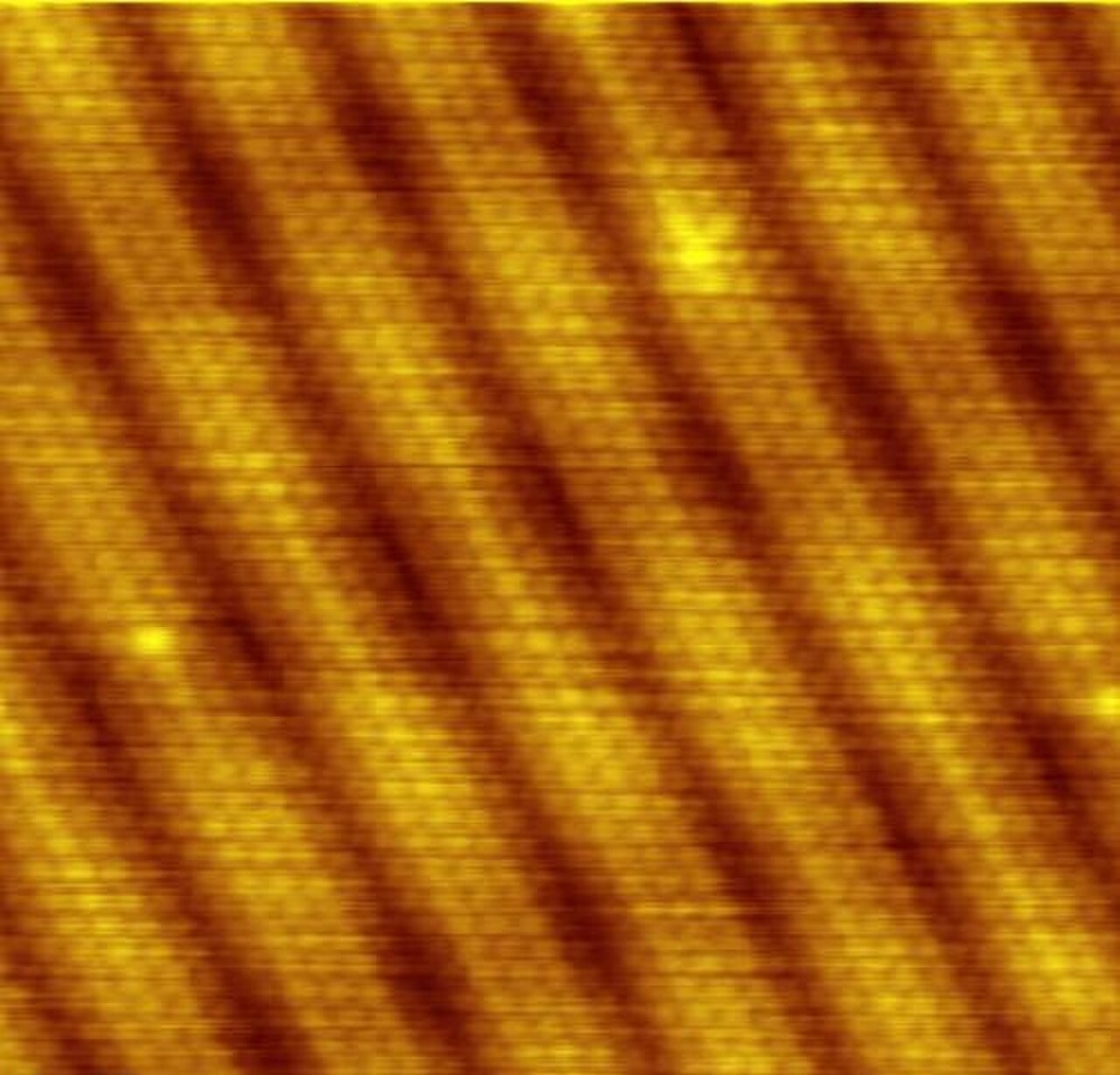
🔍 Imaging and Manipulation of Atoms: The Power of STM
The ability to image and manipulate individual atoms using Scanning Tunneling Microscopy (STM) has opened up new possibilities in nanotechnology and materials science. By using STM to manipulate individual atoms, scientists can create nanostructures with unique properties, such as quantum dots and nanowires. STM can also be used to study the properties of individual atoms and molecules, enabling a deeper understanding of their behavior and properties. For more information on the use of STM in nanotechnology, visit the National Nanotechnology Initiative website.
🤝 Relationship Between STM and Other Microscopy Techniques
The relationship between Scanning Tunneling Microscopy (STM) and other microscopy techniques is complex and multifaceted. While STM is a unique technique that enables the imaging of surfaces at the atomic level, it is often used in conjunction with other techniques, such as atomic force microscopy (AFM) and transmission electron microscopy (TEM). By combining these techniques, scientists can gain a more complete understanding of the properties of materials and surfaces. To learn more about the different microscopy techniques, visit the Wikipedia page on the topic.
📊 Future Developments and Challenges in Scanning Tunneling Microscopy
The future of Scanning Tunneling Microscopy (STM) is exciting and rapidly evolving. New developments in nanotechnology and materials science are driving the need for higher resolution and more sensitive microscopy techniques. In response, researchers are developing new variants of STM, such as spin-polarized STM and time-resolved STM. These new techniques will enable scientists to study the properties of materials and surfaces with even greater precision and accuracy. For more information on the future of STM, visit the National Science Foundation website.
📚 Conclusion: The Impact of Scanning Tunneling Microscopy on Physics and Nanotechnology
In conclusion, Scanning Tunneling Microscopy (STM) is a powerful technique that has revolutionized the field of physics and nanotechnology. By enabling the imaging of surfaces at the atomic level, STM has opened up new possibilities in materials science and surface science. As researchers continue to develop new variants of STM, we can expect to see even more exciting discoveries and innovations in the years to come. To learn more about the impact of STM on physics and nanotechnology, visit the American Physical Society website.
📊 Topic Intelligence and Key Concepts
The topic of Scanning Tunneling Microscopy (STM) is complex and multifaceted, involving concepts from quantum mechanics and solid state physics. Key ideas in STM include the concept of quantum tunneling and the use of scanning probe microscopy. Key people in the development of STM include Gerd Binnig and Heinrich Rohrer, who invented the first STM in 1981. For more information on the key concepts and people in STM, visit the Wikipedia page on the topic.
🌈 Controversy and Debates in the Field of Scanning Tunneling Microscopy
The controversy and debates surrounding Scanning Tunneling Microscopy (STM) are centered on the limitations and challenges of the technique. One of the main challenges is the need for ultra-high vacuum and low temperatures, which can limit the range of materials and surfaces that can be studied. Another challenge is the interpretation of STM images, which can be complex and require sophisticated analysis techniques. Despite these challenges, STM remains a powerful and widely used technique in nanotechnology and materials science. To learn more about the controversy and debates surrounding STM, visit the Nature website.
Key Facts
- Year
- 1981
- Origin
- IBM Zurich Research Laboratory
- Category
- Physics and Nanotechnology
- Type
- Scientific Technique
Frequently Asked Questions
What is Scanning Tunneling Microscopy (STM)?
Scanning Tunneling Microscopy (STM) is a type of scanning probe microscopy that uses a sharp conducting tip to sense the surface of materials at the atomic level. It is a powerful technique that has revolutionized the field of physics and nanotechnology. For more information on STM, visit the Wikipedia page on the topic. STM is widely used in materials science and surface science.
How does STM work?
STM works by using a sharp conducting tip to sense the surface of materials at the atomic level. The tip is brought close to the surface, allowing electrons to tunnel through the gap between the tip and the surface. This tunneling current is sensitive to the distance between the tip and the surface, enabling the imaging of surfaces at the atomic level. To understand the principles of quantum tunneling, visit the Wikipedia page on the topic. STM is often used in conjunction with other techniques, such as atomic force microscopy (AFM) and transmission electron microscopy (TEM).
What are the applications of STM?
The applications of STM are diverse and widespread. In materials science, STM is used to study the properties of materials at the atomic level, including their crystal structure and surface properties. In nanotechnology, STM is used to manipulate individual atoms and molecules, enabling the creation of nanostructures with unique properties. For more information on the applications of STM, visit the National Institute of Standards and Technology website. STM is also used in surface science to study the properties of surfaces and interfaces.
What are the limitations of STM?
The limitations of STM include the need for ultra-high vacuum and low temperatures, which can limit the range of materials and surfaces that can be studied. Another limitation is the interpretation of STM images, which can be complex and require sophisticated analysis techniques. Despite these limitations, STM remains a powerful and widely used technique in nanotechnology and materials science. To learn more about the limitations of STM, visit the Nature website. STM is often used in conjunction with other techniques, such as atomic force microscopy (AFM) and transmission electron microscopy (TEM).
Who invented STM?
The invention of STM is credited to Gerd Binnig and Heinrich Rohrer, who developed the first STM in 1981 at IBM Zürich. They were awarded the Nobel Prize in Physics in 1986 for their discovery. To learn more about the life and work of Gerd Binnig and Heinrich Rohrer, visit the Wikipedia page on the topic. The development of STM has been influenced by the work of other scientists, including Richard Feynman, who is known for his work in quantum mechanics.