Contents
- 🔌 Introduction to PCB Layout
- 💻 The History of PCB Design
- 📈 The Importance of PCB Layout in Modern Electronics
- 🔍 The PCB Design Process: From Concept to Production
- 🤖 Automation in PCB Layout: The Role of Software
- 📊 Signal Integrity and Electromagnetic Compatibility
- 🔧 Manufacturing Considerations for PCB Layout
- 🌐 The Future of PCB Layout: Trends and Innovations
- 📚 Best Practices for PCB Layout Design
- 👥 The PCB Layout Community: Resources and Forums
- 🔍 Troubleshooting Common PCB Layout Issues
- Frequently Asked Questions
- Related Topics
Overview
PCB layout is the process of designing and arranging the components and wiring of a printed circuit board. It requires a deep understanding of electronics, materials science, and manufacturing processes. With the rise of IoT and wearable technology, the demand for compact, efficient, and reliable PCBs has never been higher. However, the increasing complexity of modern electronics has made PCB layout a challenging and time-consuming task, with designers needing to balance factors such as signal integrity, thermal management, and electromagnetic interference. The use of specialized software and automation tools has improved the design process, but the need for human expertise and judgment remains. As the electronics industry continues to evolve, the importance of skilled PCB layout designers will only continue to grow, with the global PCB market projected to reach $70.4 billion by 2025, according to a report by MarketsandMarkets. The controversy surrounding the use of automated design tools versus human designers has sparked a debate about the future of the industry, with some arguing that automation will replace human designers, while others believe that human expertise will always be necessary for complex designs.
🔌 Introduction to PCB Layout
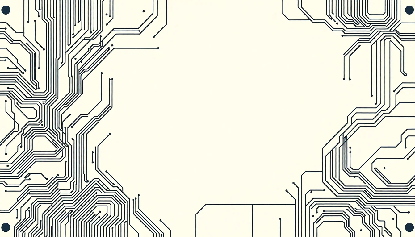
The art of PCB layout, or printed circuit board design, is a crucial aspect of electronic design that involves the careful placement and routing of components on a board. This process requires a deep understanding of electronics and circuit theory, as well as a keen eye for detail. A well-designed PCB layout can make all the difference in the performance and reliability of an electronic device, while a poorly designed one can lead to electromagnetic interference and other issues. The history of PCB design dates back to the early 20th century, when radio and telephone systems first began to use printed circuit boards. Since then, the field has evolved significantly, with advances in computer-aided design software and manufacturing techniques. For more information on the history of PCB design, see PCB design history.
💻 The History of PCB Design
The history of PCB design is a fascinating topic that involves the contributions of many inventors and engineers. One of the key figures in the development of PCB design was Paul Eisler, an Austrian engineer who patented the first PCB in 1943. Since then, the field has continued to evolve, with advances in materials science and computer science. Today, PCB design is a critical aspect of electronics manufacturing, with applications in everything from consumer electronics to aerospace engineering. For more information on the history of PCB design, see history of electronics. The use of computer-aided design software has also played a significant role in the development of PCB design, enabling designers to create complex layouts with ease and precision.
📈 The Importance of PCB Layout in Modern Electronics
The importance of PCB layout in modern electronics cannot be overstated. A well-designed PCB layout can make all the difference in the performance and reliability of an electronic device, while a poorly designed one can lead to electromagnetic interference and other issues. In addition, a good PCB layout can help to reduce electronic noise and improve signal integrity. The PCB design process typically involves several stages, including schematic capture, component placement, and routing. For more information on the PCB design process, see PCB design process. The use of simulation software can also help to identify potential issues before the board is manufactured, reducing the risk of design errors and improving overall product quality.
🔍 The PCB Design Process: From Concept to Production
The PCB design process typically involves several stages, including schematic capture, component placement, and routing. The first stage, schematic capture, involves creating a schematic diagram of the circuit using computer-aided design software. The next stage, component placement, involves placing the components on the board, taking into account factors such as thermal management and electromagnetic compatibility. The final stage, routing, involves connecting the components using copper traces. For more information on the PCB design process, see PCB design tutorial. The use of design for manufacturability techniques can also help to improve the efficiency and cost-effectiveness of the manufacturing process, reducing the risk of manufacturing defects and improving overall product yield.
🤖 Automation in PCB Layout: The Role of Software
Automation in PCB layout has become increasingly important in recent years, with the use of computer-aided design software and artificial intelligence algorithms to improve the efficiency and accuracy of the design process. One of the key benefits of automation in PCB layout is the ability to reduce design errors and improve product quality. For more information on automation in PCB layout, see automated PCB design. The use of machine learning algorithms can also help to optimize the design process, reducing the time and effort required to create a high-quality PCB layout. Additionally, the use of collaboration tools can help to improve communication and coordination between designers, manufacturers, and other stakeholders, reducing the risk of miscommunication and improving overall project management.
📊 Signal Integrity and Electromagnetic Compatibility
Signal integrity and electromagnetic compatibility are critical considerations in PCB layout, as they can have a significant impact on the performance and reliability of an electronic device. Signal integrity refers to the ability of a signal to maintain its integrity and accuracy as it travels through the circuit, while electromagnetic compatibility refers to the ability of a device to operate in the presence of other electronic devices without interference. For more information on signal integrity and electromagnetic compatibility, see signal integrity tutorial. The use of shielding and filtering techniques can help to reduce electromagnetic interference and improve signal integrity, while the use of grounding and bonding techniques can help to improve electromagnetic compatibility. The selection of components with high signal-to-noise ratio and low electromagnetic interference can also help to improve signal integrity and electromagnetic compatibility.
🔧 Manufacturing Considerations for PCB Layout
Manufacturing considerations are critical in PCB layout, as they can have a significant impact on the cost, quality, and reliability of the final product. Design for manufacturability techniques can help to improve the efficiency and cost-effectiveness of the manufacturing process, reducing the risk of manufacturing defects and improving overall product yield. For more information on manufacturing considerations, see PCB manufacturing. The use of standard operating procedures and quality control techniques can also help to ensure that the manufacturing process is consistent and reliable, reducing the risk of quality issues and improving overall customer satisfaction. The selection of materials with high thermal stability and low moisture absorption can also help to improve the reliability and durability of the final product.
🌐 The Future of PCB Layout: Trends and Innovations
The future of PCB layout is likely to be shaped by advances in artificial intelligence, internet of things, and 5G technologies. One of the key trends in PCB layout is the increasing use of automation and machine learning algorithms to improve the efficiency and accuracy of the design process. For more information on the future of PCB layout, see future of PCB design. The use of cloud computing and collaboration tools can also help to improve communication and coordination between designers, manufacturers, and other stakeholders, reducing the risk of miscommunication and improving overall project management. The development of new materials and components with high signal-to-noise ratio and low electromagnetic interference can also help to improve the performance and reliability of electronic devices.
📚 Best Practices for PCB Layout Design
Best practices for PCB layout design involve a combination of technical skills and attention to detail. One of the key best practices is to use computer-aided design software to create a schematic diagram of the circuit and to simulate the behavior of the circuit before manufacturing. For more information on best practices for PCB layout design, see PCB design best practices. The use of design for manufacturability techniques can also help to improve the efficiency and cost-effectiveness of the manufacturing process, reducing the risk of manufacturing defects and improving overall product yield. The selection of components with high signal-to-noise ratio and low electromagnetic interference can also help to improve the performance and reliability of electronic devices. Additionally, the use of version control and documentation techniques can help to ensure that the design process is well-documented and easy to follow, reducing the risk of design errors and improving overall product quality.
👥 The PCB Layout Community: Resources and Forums
The PCB layout community is a vibrant and active community of designers, manufacturers, and other stakeholders who share knowledge, resources, and best practices. One of the key resources for the PCB layout community is the PCB design forum, where designers can ask questions, share tips, and learn from others. For more information on the PCB layout community, see PCB community. The use of social media and collaboration tools can also help to improve communication and coordination between designers, manufacturers, and other stakeholders, reducing the risk of miscommunication and improving overall project management. The development of new tutorials and training programs can also help to improve the skills and knowledge of PCB layout designers, reducing the risk of design errors and improving overall product quality.
🔍 Troubleshooting Common PCB Layout Issues
Troubleshooting common PCB layout issues is a critical skill for any PCB layout designer. One of the key issues is electromagnetic interference, which can cause a range of problems, from signal integrity issues to system crashes. For more information on troubleshooting common PCB layout issues, see PCB troubleshooting. The use of debugging tools and simulation software can help to identify and fix issues before the board is manufactured, reducing the risk of design errors and improving overall product quality. The selection of components with high signal-to-noise ratio and low electromagnetic interference can also help to improve the performance and reliability of electronic devices. Additionally, the use of testing and validation techniques can help to ensure that the PCB layout is correct and functional, reducing the risk of design errors and improving overall product quality.
Key Facts
- Year
- 1960
- Origin
- The first PCBs were developed in the 1960s by companies such as IBM and Bell Labs, with the first commercial PCBs being produced in the early 1970s.
- Category
- Electronics and Engineering
- Type
- Technical Concept
Frequently Asked Questions
What is PCB layout?
PCB layout, or printed circuit board design, is the process of creating a physical layout for a printed circuit board. This involves placing and routing components on the board, taking into account factors such as signal integrity, electromagnetic compatibility, and thermal management. For more information on PCB layout, see PCB layout. The use of computer-aided design software can help to improve the efficiency and accuracy of the design process, reducing the risk of design errors and improving overall product quality.
What are the benefits of good PCB layout?
Good PCB layout can improve the performance and reliability of an electronic device, reduce electromagnetic interference, and improve signal integrity. For more information on the benefits of good PCB layout, see PCB layout benefits. The use of design for manufacturability techniques can also help to improve the efficiency and cost-effectiveness of the manufacturing process, reducing the risk of manufacturing defects and improving overall product yield.
What are the common mistakes in PCB layout?
Common mistakes in PCB layout include poor signal integrity, electromagnetic interference, and thermal management issues. For more information on common mistakes in PCB layout, see PCB layout mistakes. The use of simulation software can help to identify and fix issues before the board is manufactured, reducing the risk of design errors and improving overall product quality.
How do I learn PCB layout?
You can learn PCB layout by taking online courses, attending workshops, and practicing with computer-aided design software. For more information on learning PCB layout, see PCB layout tutorial. The use of tutorials and training programs can also help to improve the skills and knowledge of PCB layout designers, reducing the risk of design errors and improving overall product quality.
What are the tools used in PCB layout?
The tools used in PCB layout include computer-aided design software, simulation software, and manufacturing equipment. For more information on the tools used in PCB layout, see PCB layout tools. The use of collaboration tools can also help to improve communication and coordination between designers, manufacturers, and other stakeholders, reducing the risk of miscommunication and improving overall project management.